(China (Mainland))

Product Summary
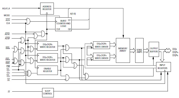
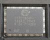
The CY7C1324F-133AC is a 131,072 x 18 synchronous cache RAM designed to interface with high-speed microprocessors with minimum glue logic. Maximum access delay from clock rise is 6.5 ns (133-MHz version). A 2-bit on-chip counter captures the first address in a burst and increments the address automatically for the rest of the burst access. The CY7C1324F-133AC operates from a +3.3V core power supply while all outputs may operate with a +3.3V supply. All inputs and outputs are JEDEC-standard JESD8-5-compatible.
Parametrics
CY7C1324F-133AC absolute maximum ratings: (1)Storage Temperature : –65°C to +150°C; (2)Ambient Temperature with Power Applied: –55°C to +125°C; (3)Supply Voltage on VDD Relative to GND: –0.5V to +4.6V; (4)DC Voltage Applied to Outputs in Three-State : –0.5V to VDDQ + 0.5V, DC Input Voltage: –0.5V to VDD + 0.5V; (5)Current into Outputs (LOW): 20 mA; (6)Static Discharge Voltage: >2001V; (7)Latch-up Current: >200 mA.
Features
CY7C1324F-133AC features: (1)128K x 18 common I/O; (2)3.3V –5% and +10% core power supply (VDD); (3)3.3V I/O supply (VDDQ); (4)Fast clock-to-output times 6.5 ns (133-MHz version), 7.5 ns (117-MHz version); (5)Provide high-performance 2-1-1-1 access rate; (6)User-selectable burst counter supporting Intel Pentium interleaved or linear burst sequences; (7)Separate processor and controller address strobes; (8)Synchronous self-timed write; (9)Asynchronous output enable; (10)Supports 3.3V I/O level; (11)Offered in JEDEC-standard 100-pin TQFP package; (12)ZZ Sleep Mode option.
Diagrams